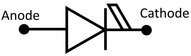
1. Theory
- Definition: A PIN diode has a wide, lightly doped (nearly intrinsic) i-layer sandwiched between heavily doped and regions.
- Intrinsic layer: The i-region’s residual doping is so low that it fully depletes at a small reach-through voltage, so its physical thickness fixes the depletion width.
- Uniform field: The field across the depleted i-region is nearly uniform rather than triangular, so breakdown voltage scales roughly linearly with i-layer thickness.
- Conductivity modulation: Under forward bias, electrons and holes injected from both ends flood the i-region as a dense plasma, greatly lowering its resistance.
- Stored charge: The forward current sustains a stored charge in the i-region, set by the forward current and the ambipolar carrier lifetime.
2. Working Principle
- Reverse bias: Beyond reach-through the i-region is fully depleted, giving a small, nearly bias-independent capacitance; at RF the diode looks like a small capacitor (off state).
- Forward bias: The injected plasma gives a current-controlled resistance that falls inversely with forward current (on state).
- RF behaviour: When the carrier lifetime is much longer than the RF period, the stored charge cannot follow the signal, so the diode does not rectify and acts as a linear resistor set by the DC bias.
- High breakdown: The wide, uniformly stressed i-layer supports large reverse voltages.
- Switching trade-off: A long lifetime lowers on-resistance, but more stored charge must be removed at turn-off, increasing the reverse recovery time.
- Photodetection: Photons absorbed in the wide depleted i-region create electron-hole pairs that are swept out by drift, giving high quantum efficiency and fast response.
3. Applications
- RF and microwave switches: Standard high-power switching element for antenna and transmit-receive switching.
- Variable attenuators and phase shifters: Bias-controlled RF resistance gives continuous attenuation and phase control.
- RF limiters: Self-biased PIN diodes protect sensitive receiver inputs from high-power signals.
- Photodiodes: Main detector in fibre-optic receivers, where speed and efficiency matter.
- High-voltage power rectifiers: The -- structure is the basis of bipolar power rectifiers at voltages too high for Schottky diodes.
- Radiation detectors: Fully depleted silicon PIN diodes detect X-rays and charged particles.
| Name | Formula | Related Formulae | Variables/Constants |
|---|---|---|---|
| Built-in potential (contact potential) | |||
| Reach-through (full depletion) voltage | |||
| Depletion (junction) capacitance | |||
| Stored charge in the intrinsic region (forward bias) | |||
| Forward (charge-controlled) resistance of the i-region | |||
| Carrier transit time across the i-region | |||
| RF cutoff frequency | |||
| Reverse breakdown voltage (near-uniform field approximation) | |||
| Reverse recovery time |
Important Questions
Ques: Why is PIN diode junction capacitance nearly constant with reverse bias, unlike a standard PN diode?
In a PN step junction, because the depletion width keeps growing into both doped regions as reverse bias increases. In a PIN diode, the lightly doped “intrinsic” layer has such a low residual doping that it fully depletes at a very small reach-through voltage ; beyond that point, the depletion region is pinned at the fixed physical width of the i-layer and cannot grow any further (the heavily doped and regions barely deplete at all), so stays essentially constant over the diode’s entire useful reverse-bias range. This near-constant, deliberately low capacitance is precisely why PIN diodes are chosen over PN diodes for RF and microwave applications. Reference: S.M. Sze and Kwok K. Ng, Physics of Semiconductor Devices, 3rd ed., Wiley, 2007.
Ques: Why does a PIN diode behave like a variable resistor under forward bias instead of following the exponential Shockley I-V law like a PN diode?
Under forward bias, electrons and holes are injected into the intrinsic region in roughly equal, high concentrations (an ambipolar plasma), since there is no background doping to set a fixed majority-carrier population the way there is in a conventional PN diode’s quasi-neutral regions. The resulting conductivity of the i-region is set by this injected carrier density, which in turn is controlled by the forward current through the stored charge , giving a resistance that varies smoothly and continuously with rather than exhibiting the sharp exponential turn-on of a conventional diode junction. This charge-controlled-resistance behavior is exactly what makes PIN diodes useful as electronically variable RF attenuators and switches. Reference: S.M. Sze and Kwok K. Ng, Physics of Semiconductor Devices, 3rd ed., Wiley, 2007; general RF/microwave PIN diode switch design references.
Ques: Why does PIN diode breakdown voltage scale roughly linearly with instead of the quadratic-in-doping relation used for a step junction?
Because the field across a fully depleted, lightly doped i-region is nearly uniform (rather than triangular and sharply peaked as in a one-sided step junction), the breakdown condition is reached when that nearly-constant field equals the critical field across the entire width , giving — a linear relationship. This is the key structural advantage of the PIN diode: widening the intentionally undoped i-layer buys roughly proportional increases in breakdown voltage without the steep doping-dependent tradeoffs a step junction faces, which is why PIN structures are also used in high-voltage power rectifiers and photodiodes, not just RF switches. Reference: S.M. Sze and Kwok K. Ng, Physics of Semiconductor Devices, 3rd ed., Wiley, 2007.
Related pages in this vault: Schottky Diode, PN Junction, GaN Power Diode, Step Recovery Diode, PIN Photodiode, Diodes (PN, PIN, Schottky, Zener), Silicon Carrier-Injection PIN Modulator, Power Device Compact Models, Diode Compact Models.