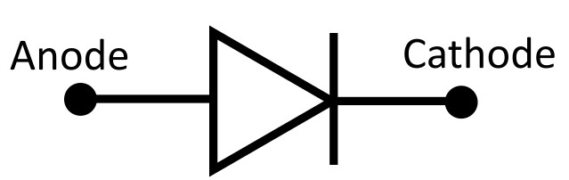
1. Theory
- Definition: A PN junction is the boundary formed when P-type and N-type regions are created within one continuous semiconductor crystal.
- Carrier diffusion: The concentration gradient drives holes from the P-side into the N-side and electrons from the N-side into the P-side, where they recombine.
- Depletion region: Diffusion leaves behind immobile ionized acceptors (negative) on the P-side and ionized donors (positive) on the N-side, forming a region almost free of mobile carriers.
- Built-in potential: The space charge sets up an electric field and a contact potential that opposes further diffusion; at equilibrium, drift and diffusion currents balance and the Fermi level is flat across the junction.
- Doping asymmetry: The depletion region extends further into the more lightly doped side, so in a one-sided junction it lies almost entirely in that side.
2. Working Principle
- Zero bias: Diffusion and drift currents cancel, so no net current flows.
- Forward bias: A positive voltage on the P-side lowers the barrier, narrows the depletion region and injects minority carriers that diffuse and recombine, so current rises exponentially with voltage.
- Cut-in voltage: Significant conduction begins at roughly 0.6–0.7 V for Si and about 0.3 V for Ge.
- Reverse bias: The barrier rises and the depletion region widens; only a small, nearly voltage-independent saturation current from thermally generated minority carriers flows.
- Capacitance: Depletion capacitance dominates under reverse bias, while diffusion (stored-charge) capacitance dominates under forward bias.
- Switching: Stored minority charge must be removed when switching from forward to reverse bias, which sets the reverse recovery time.
- Breakdown: Beyond a critical reverse voltage, current rises sharply through avalanche multiplication or Zener tunnelling.
3. Applications
- Rectification: Converts AC to DC in half-wave and full-wave rectifiers.
- Signal detection: Demodulates AM and other RF signals.
- Clipping and clamping: Limits or shifts signal levels in waveform-shaping circuits.
- Switching and protection: Used for signal steering, reverse-polarity protection and freewheeling across inductive loads.
- Device building block: Forms the basis of BJTs, JFETs, LEDs, photodiodes, solar cells and most other devices in this vault.
| Name | Formula | Related Formulae | Variables/Constants |
|---|---|---|---|
| Built-in potential (contact potential) | |||
| Depletion region width | |||
| Maximum electric field | |||
| Depletion (junction) capacitance | |||
| Debye length | |||
| Ideal diode equation (Shockley law) | |||
| Reverse saturation current | |||
| Excess minority carrier concentration (injection profile) | |||
| Diffusion (charge-storage) capacitance | |||
| Total diode capacitance | |||
| Small-signal (dynamic) diode resistance | |||
| Reverse breakdown voltage (one-sided step junction) | |||
| Temperature dependence of saturation current | |||
| Reverse recovery time |
Important Questions
Ques: Why does the ideal diode equation use rather than a more general injection model?
The Shockley diode equation follows directly from solving the minority-carrier diffusion equation with the “law of the junction” boundary condition, which fixes the minority carrier concentration at each depletion edge to and under the assumption of low-level injection (injected minority carriers remain much smaller than the majority carrier concentration) and negligible recombination within the depletion region itself. When these assumptions break down — high injection levels, or significant generation-recombination current inside the depletion region — the ideality factor deviates from 1 (commonly approaching 2 for recombination-dominated current), which is why is carried as an explicit parameter rather than fixed at unity. Reference: S.M. Sze and Kwok K. Ng, Physics of Semiconductor Devices, 3rd ed., Wiley, 2007; D.A. Neamen, Semiconductor Physics and Devices, 4th ed., McGraw-Hill, 2012.
Ques: Why does junction capacitance dominate under reverse bias while diffusion capacitance dominates under forward bias?
Junction (depletion) capacitance arises from the fixed ionized dopant charge exposed on either side of the depletion region, and it exists and is meaningful under both bias directions; but under forward bias, injected minority carriers accumulate as stored charge that grows exponentially with (mirroring the diode current itself), and this diffusion capacitance quickly outgrows the depletion capacitance because it scales with rather than the much weaker dependence of . This is why depletion capacitance is the relevant design parameter for reverse-biased applications (e.g. varactor diodes), while diffusion capacitance sets the switching-speed limit of a forward-biased diode. Reference: S.M. Sze and Kwok K. Ng, Physics of Semiconductor Devices, 3rd ed., Wiley, 2007.
Ques: Why is reverse breakdown voltage included on the general PN junction page instead of only on the Zener/Avalanche pages?
Every PN junction has a finite breakdown voltage set by its doping and geometry, whether or not the device is intended to be operated there — the formula above describes when avalanche multiplication begins for a generic one-sided step junction, which is fundamental diode behavior, not a special-purpose feature. The dedicated Zener and Avalanche diode pages will go further into the physical multiplication mechanism (impact ionization, multiplication factor ) and the doping-dependent transition between Zener (tunneling-dominated, low voltage, heavily doped) and true avalanche breakdown (impact-ionization-dominated, higher voltage), building directly on this baseline relationship. Reference: S.M. Sze and Kwok K. Ng, Physics of Semiconductor Devices, 3rd ed., Wiley, 2007.
Ques: What is the Debye length used for in the context of a PN junction?
The Debye length is the characteristic distance over which mobile carriers screen out an internal electric field, and the standard “depletion approximation” used to derive , , and above is only valid when the depletion width is much larger than the Debye length () — otherwise the assumption of an abrupt boundary between a fully depleted region and a field-free neutral region breaks down, and the junction’s actual carrier and field profiles become smoother than the idealized step-junction picture. This condition is comfortably satisfied for typical doping levels in Si and III-V diodes, which is why the depletion approximation is used so freely in practice, but it becomes a real limitation for very heavily doped or very narrow junctions. Reference: S.M. Sze and Kwok K. Ng, Physics of Semiconductor Devices, 3rd ed., Wiley, 2007.
Related pages in this vault: Schottky Diode, Zener Diode, PIN Diode, Backward Diode, Diode-Type Selector (PN and Schottky), Basic Semiconductor Equations, PN Photodiode, Diodes (PN, PIN, Schottky, Zener), Diode Compact Models, Generation-Recombination Models, Light Emitting Diode (Homojunction and Heterojunction LED), Solar Cell Fundamentals, LCR Meter and C-V, Silicon Carrier-Depletion Mach-Zehnder Modulator.